Trace Aesthetics
Published on 2017-09-18 in Fritzing Tricks.
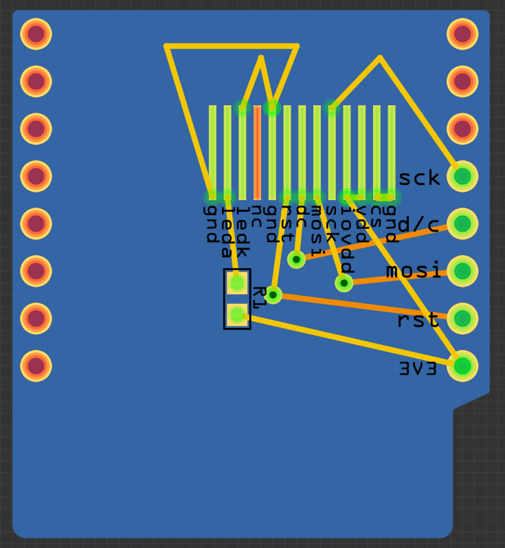
I’ve been putting this post off for some time now, but we need to talk about this sooner or later. Fritzing became infamous in the electronics community for the characteristic ugly traces that are often done with it. People new to the whole thing just connect the holes and pads in straight lines, adding a bend sometimes when necessary, and call it a day. It looks something like this:

What’s wrong with this, you ask? All the connections are there, so it will work fine, after all, no?
Well, there is a number of things wrong. First of all, you are just being lazy, and that’s a sure warning sign that most likely there will be other problems with this design. Second, this is not pleasant to look at, and more importantly, to work with. It’s not easy to see what is connected where and to modify this design. It’s also easy to miss shorts between the traces. Finally, there are actual technical reasons why this design is sub-optimal.
You probably have heard about radio-frequency emissions from traces. Turns out that every trace is basically a small antenna, and it will waste energy by emitting radio waves. Most traces are not particularly good antennas, but the ones that have a lot of sharp angles and are not surrounded by copper fill are better at emitting noise. Unless you are working with gigahertz signal, this is not the technical reason for worrying about sharp angles, though.
If you are etching your own boards, you have to be very careful about all the nooks and crannies in your design. The etchant will tend to pool int them, and eat out much more copper in those places, leading to possible faulty boards. This is not the technical reason for worrying about sharp angles if you send your design to a professional board house for fabrication, though. Neither is the fact that because of the lack of a copper fill, a lot of copper has to be etched away and a lot of the etchant wasted on that, and the etching process will take a lot of time.
Finally, the sharp corners are more likely to peel off the board, especially if it’s subject to any mechanical stresses or bad storage. Again, not much of an issue with professionally made boards.
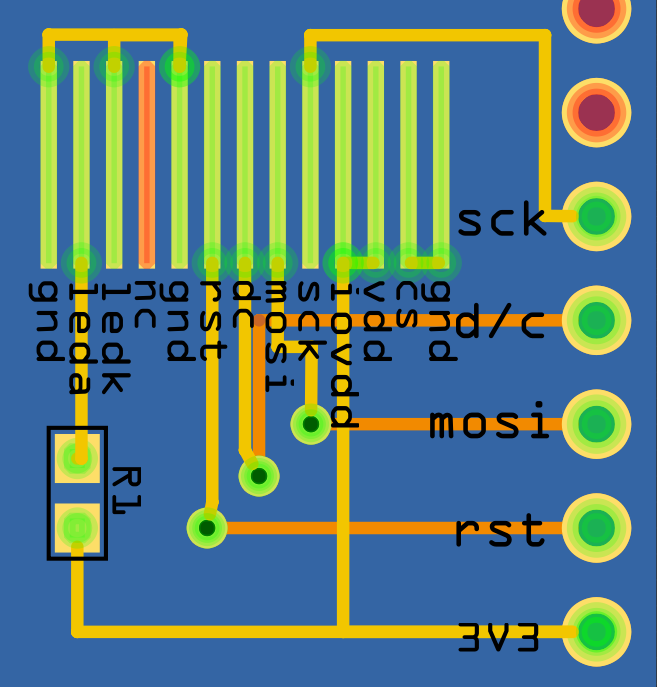
But it still looks very bad, and all the people who ate their teeth on the above-mentioned limitations will shudder at the sight of it. So please, be a nice person and spend the minimal extra effort to actually make it look good. Start by aligning all the traces so that you only have horizontal, vertical and diagonal lines (you can hold ctrl+shift while moving the trace for Fritzing to help you with it):

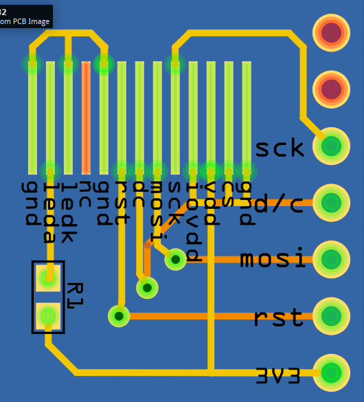
Much better already, don’t you think? Now let’s get rid of those sharp
angles:

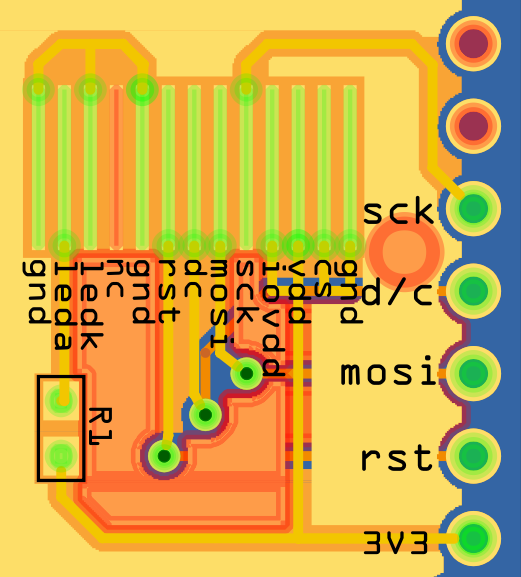
It’s starting to look right, doesn’t it? Note that I actually left a couple of right angles in there — in the T-junctions, and also for the traces that are too close together to actually do a nice gradual turn. Personally I think this is fine, but for the reasons I listed above, opinions vary. Finally, let’s add a copper fill:

Et voila! A decent looking PCB design. It wasn’t so difficult after all, was it?
Of course there is much more to it than just the horizontal and vertical lines and sharp angles. But this is already a start. If you keep practicing, looking at other people’s designs, etc. you will come up with your own set of good habits that make the designs nicer, easier to read, less likely to contain mistakes, and more pleasant to work with.
 deshipu.art