My Way
Published on 2021-06-23 in Home Button for Keyboards.
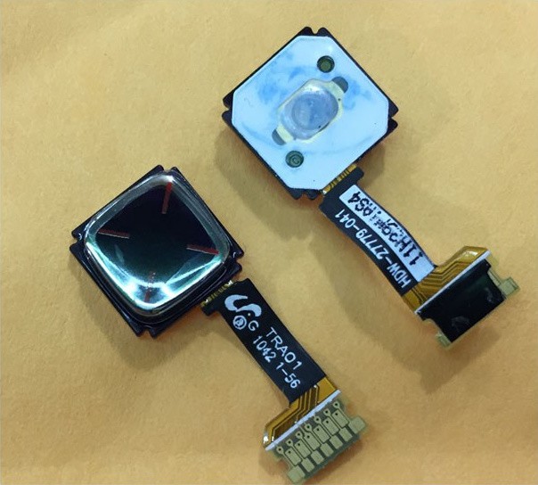
I decided that the sensor from a Blackberry 8520 has too fancy a connector, which would be difficult to source and to solder (with a 0.4mm pitch), so I looked at other similar sensors, and picked one from a Blackberry 9300. Originally it no doubt uses even fancier connector, but the sensor-side is just a piece of flex PCB with a bunch of pads on it — something that should be easy enough to solder directly to a PCB.

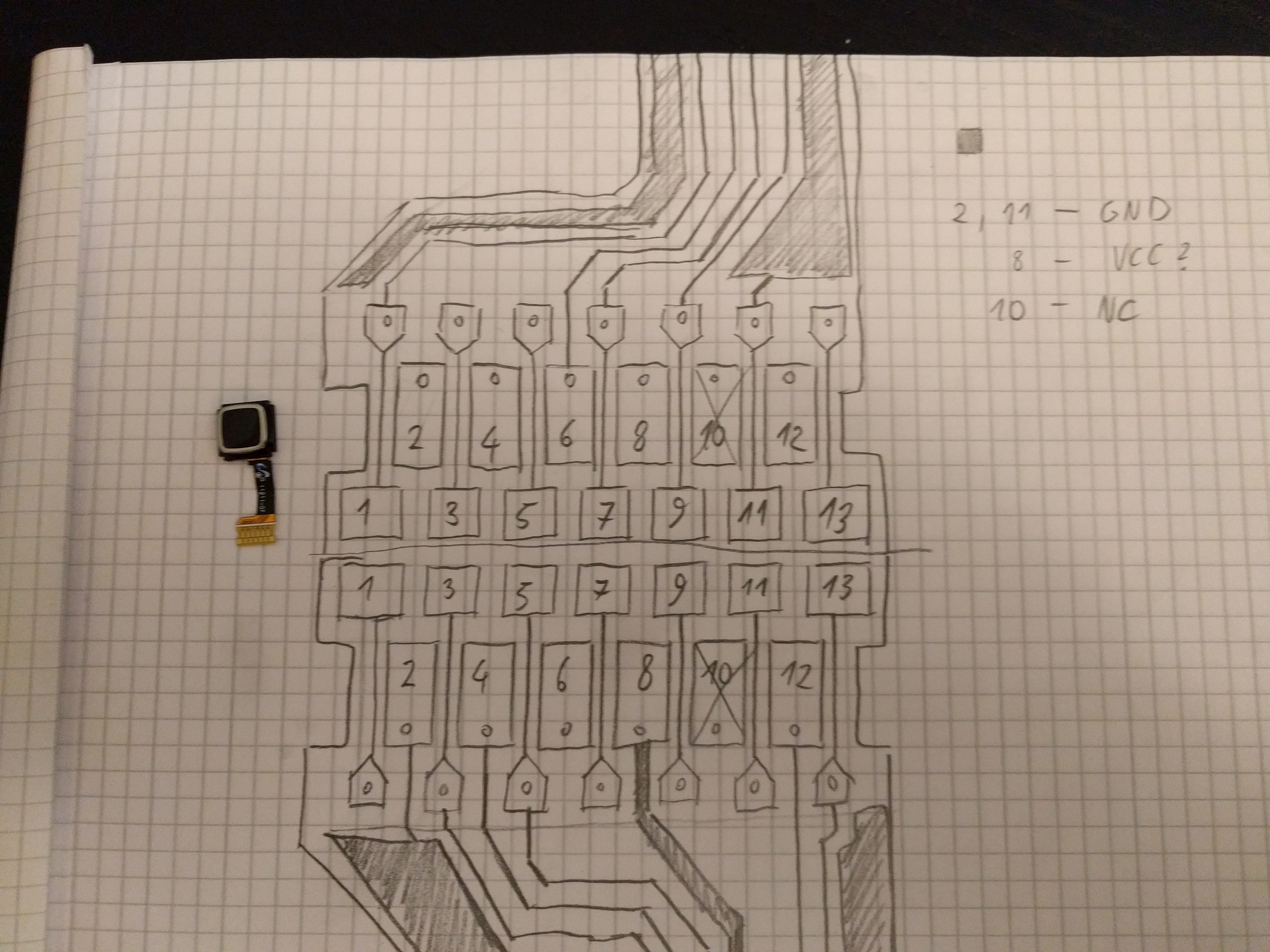
So I got a pair of those, and got to work on them. The initial probing yielded me this:

GND was easy to find, because it is connected with the ground fill on the flex PCB. The VCC was easy too, because it’s the only track that is thicker than all the others. And finally pin 10 is not connected, which was easy to figure out by visual inspection — there are no traces going to it!
Next, I got out an ohmmeter and found that pins 12 and 13 are connected to the tact switch on the bottom of the sensor. That is 6 out of 13 pins out of the way, 7 more left to go.
Those remaining pins should be, if this sensor is similar to the other one, CS, SCK, MISO, MOSI, RESET, SHUTDOWN, and INTERRUPT (aka MOVEMENT). There are lots of possible combinations here, but if you look carefully at the traces, you will note that they are in fact bundled in two distinct groups. My bet is that one of those groups is going to be all the SPI pins, and the other — the rest.
Well, we won’t know until we try. So the next step was soldering some wires to those pads, to connect them to a microcontroller and try sending some signals. Unfortunately, it turns out that the pads are way to small to do that, and soldering to a flex PCB is way too hard. After a few failed attempts, I decided to make a custom PCB with a footprint matching those pads. That delays the project a little bit.
 deshipu.art